- Home >> Solution >> IOT >> smart home
Smart home controller hardware module solution
The smart home smart controller adopts the embedded system design method. In terms of hardware design, try to choose universal and modular equipment, divide the hardware functions according to the system equipment, and unify the interface, so as to increase the versatility and practicability of each module and facilitate system maintenance and upgrading.
1. The hardware structure of the smart home system controller
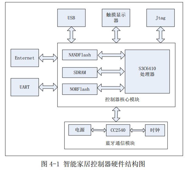
According to the different functions of hardware devices, the hardware of smart home smart controllers can be roughly divided into microprocessors, peripheral circuits to ensure the normal operation of the system, input and output devices, communication modules, etc. Among them, the microprocessor of the smart home controller adopts the Samsung S3C6410ARM processor designed to provide low-cost solutions for smart terminals, and is equipped with peripheral circuits such as power modules to ensure its work. The input and output devices are touch screens that are commonly used in intelligent terminal products. The communication module includes an Ethernet interface module, a bluetooth module and a serial communication module. The most important part of the system is to expand the low-power bluetooth module, so that the controller can realize the control of smart home devices through bluetooth communication. The hardware system structure of the smart home controller is shown in Figure 4-1.

2. Core module design of smart home controller
The core module of the smart home controller is centered on the S3C610 processor, equipped with some necessary peripheral circuits, such as power supply module, clock and reset module, etc., to form the minimum system for the controller to operate. And it expands the memory module and the JTAG interface module used for system debugging.
2.1 Power module
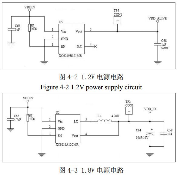
The power module is the basis of the entire controller system and plays a very important role, but it is also a part that is often overlooked by many developers. The external power supply used in this program is 5V, and the 1.2V voltage required by the microprocessor is obtained through the management of the power supply circuit; the 1.8V voltage required by DDR SDRAM, etc.; the 3.3V voltage required by the Bluetooth module, USB, and serial port; the required voltage by the touch display 5V voltage. Figure 4-2 and 4-3 are the design of 1.2V power supply circuit and 1.8V power supply circuit respectively.

Among them, XC9216A12CMR is a step-down DC/DC converter with synchronous rectification, built-in 0.6Ω P-Channel MOSFET switch and 0.7Ω N-Channel MOSFET switch.
XC9216A12CMR has a very high operating frequency so that the circuit can use very small inductance and capacitance. Usually two ceramic capacitors and an inductor can be used to build an output line up to 500mA.
2.2 Clock reset module
(1) Clock module: The clock signal is generally generated by a quartz crystal oscillator, and the required clock signal can be obtained by configuring it as required. S3C6410 has a clock oscillation circuit, and a 48MHz crystal oscillator can be connected between the XUSBTI and XUSBXTO pins of the chip to make it work normally. Under 1.2V voltage, its operating frequency can reach 667MHz. If the system needs a higher operating frequency, you can use the PPL provided by the S3C6410. Theoretically, the operating frequency can be multiplied to 1.6GHz.
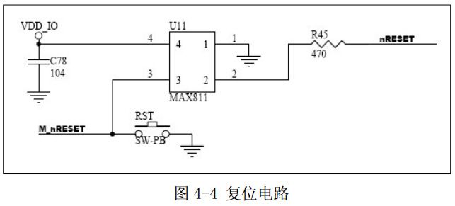
(2) Reset module: The working state of the embedded microprocessor is usually unstable when it is first powered on, which affects the microprocessor so that it cannot work normally. In order to enable the microprocessor to return to a certain working state at any time, it is necessary to design a reset circuit for it. The reset control signal should be based on the input and output voltage of the pin of the microprocessor as a reference. The pin voltage range of S3C6410 is 3.0V~3.6V, so the threshold voltage of the general control signal is less than 3.0V. The circuit provides physical buttons, so that the system can realize the functions of power-on reset and artificial button reset when the system is working. Figure 4-4 shows the reset circuit design of the system.

The reset circuit uses the MAX811 chip. The MAX811 is a reliable and low-cost digital system power monitoring chip. Its operating voltage is 5V or 3V, and the power threshold is 2.93V. These characteristics can meet the needs of the system.
2.3 Storage module
(1) SDRAM interface circuit: SDRAM needs a synchronous clock to work, and the memory array must be continuously refreshed in order not to lose data. Once the power is off, the stored data will be lost. Because S3C6410 supports the mobile SDRAM interface of 32-bit data bus, so this system adopts two mobile DDR SDRAMs whose model is K4XIG163PC-FGC6. The power supply of K4XIG163PC-FGC6 of mobile DDR SDRAM is 1.8V, the power consumption is relatively low, and it supports sleep function, and the work does not need pull-up resistors. The design is simple and convenient. K4XIG163PC-FGC6 has four Banks, each Bank corresponds to 32 bytes (16Mbit X 16). So the total SDRAM size of the system is 256M.
(2) NAND-Flash interface circuit: NAND-Flash is a kind of Flash memory, and its implementation mode uses a nonlinear macro-unit scheme, which provides a low-cost solution for solid-state large-capacity memory. S3C6410 supports the NAND-Flash interface of 8-bit data bus, and the NAND-Flash of this solution uses K9F2G08. The storage capacity of K9F2G08 is 1 Gbit, and the bit width is 8 bits. The page size is 1 028×4 bit, each block is composed of 64 pages, and there are 2048 blocks in total. The working voltage of K9F2G08 is 2.7V~3.6V. The XSELNAND pin of S3C6410 is directly connected to VDD_IO, and the high level indicates that the Flash selection type is NAND-Flash.
2.4 JTAG interface module
The full name of JTAG is "Joint Test Action Group", which is a standard test protocol widely used in internal testing of chips and system simulation debugging. General FPGA, ARM, DSP and other chips all support JTAG. This system provides JTAG module, which is convenient for developing and debugging the system.
3. Design of communication module of smart home controller
The smart home controller is responsible for controlling the internal LAN communication of the home, and the external network uses it to access and control the internal equipment of the home. Therefore, the smart home controller must have the necessary communication interface modules. The communication module of the smart home controller designed in this scheme includes: Ethernet interface module, which is responsible for accessing the external network; Bluetooth communication module, which is the communication interface of the home's internal LAN; Used during testing and debugging.
3.1 Ethernet interface module
Ethernet (Ethernet) refers to the baseband LAN specification proposed by Xerox, and then developed under the joint development of Xerox, DEC, and Intel. This communication protocol standard is the most common in existing LAN applications. At present, the standard technology is very mature, and there are abundant products and development tools on the market. The Ethernet interface chip used in this system is DM9000AEP, which has a 10/100M adaptive transceiver and 4K double-word SRAM. The chip is a highly integrated high-speed Ethernet MAC controller with low power consumption, high speed, and compatibility with 5.0V and 3.3V input and output voltages.
3.2 USB Host module
USB (Universal Serial BUS) is a bus standard used to regulate the connection and communication between computers and peripherals. USB devices support hot-swapping and plug-and-play functions. The smart home controller designed in this paper is conducive to the expansion and communication of external devices. Among them, the communication between the Bluetooth module controlled by the smart home and the host is realized through the USB interface. Devices in USB communication are divided into two types: USB Host (master device) and USB Slave (slave device). S3C6410 supports USB host devices with 2 ports, and integrates all components of the USB controller, and the peripheral circuit design is relatively simple and easy to implement.
3.3 Bluetooth communication module
Since the Bluetooth 4.0 protocol was officially adopted in 2010, there are not many chips that support the low-power Bluetooth 4.0 protocol in the market, mainly including the new generation of low-power Bluetooth chip nRF8001 launched by Nordic and the low-power Bluetooth chip of TI. CC2540. As the first complete low-power Bluetooth chip, CC2540 is currently a highly integrated ANT wireless network processor, designed for ultra-low-power short-range wireless communication for consumer electronics, mobile accessories, and sports medical applications. plan. A system-on-chip using CC2540 Bluetooth can generally work continuously for several months or even more than a year with only one button battery. Therefore, from the perspective of reliability and practicability, this system uses CC2540 as a low-power bluetooth solution. CC2540 integrates enhanced C8051 single-chip core and RF front-end on a single chip, which has a higher computing speed. It has two common asynchronous/synchronous serial communication interfaces USART; the chip has a hardware multiplier, which enhances the data processing and computing capabilities. The communication current consumption of CC2540 is 19.6mA~24mA, and it has good compatibility and interoperability with other frequency 2.4GHz communication devices, and complies with the latest Bluetooth protocol specification version 4.0 low power consumption mode.
3.4 Serial communication module
Serial port communication is a common communication method on computer equipment. Equipped with a serial communication module on the smart home controller can facilitate the expansion of serial devices, and at the same time facilitate the development and debugging of the system. At present, the commonly used asynchronous serial communication interfaces mainly include RS-232 interface, RS-449 interface and RS485 interface. S3C6410 supports the sending and receiving of 5-bit, 6-bit, 7-bit or 8-bit serial data. This solution adopts the RS-232-C interface standard based on RS-232. This standard is equipped with 25 signal lines, including a main channel and an auxiliary channel. The working voltage is between plus and minus 3~15V, so no external The power supply equipment meets the requirements of this system.
4. Design of input and output modules of smart home controller
At present, the most widely used human-computer interaction devices on embedded smart terminals include LCD monitors and touch input screens. This solution uses the above two devices as input and output devices, and with the Android operating system, it can make the smart home controller easy to use and has a better user experience.
4.1 LCD display module
S3C6410 integrates LCD controller inside and supports typical screen sizes: 800×480, 640×480, 320×240. The smart home controller designed in this paper considers to reduce the cost as much as possible without affecting the use, and adopts NEC's 4.3-inch TFT LCD display with a touch screen. This display has a relatively high cost performance, and supports true color display, and the color is adjustable. This meets the requirements of S3C6410.
4.2 Touch screen module
The more common touch screens are resistive, capacitive, infrared and surface acoustic wave touch screens. Among them, the resistive touch screen has better stability, the response sensitivity can meet the requirements, and the price is cheap, so this paper adopts the four-wire resistive touch screen as the solution of the input device. The touch screen screen is composed of two parts, the vertical resistance line and the horizontal resistance line. S3C6410 controls the on or off of the four MOS tubes through the four pins X+, X-, Y+, and Y- of the touch screen, so that the X coordinate and Y coordinate of the touch screen can be read in time-sharing to determine the input position. Before the system starts to use, the position of the touch screen must be corrected by five-point correction.
Summarize
Through the above-mentioned design of each module, the hardware design work of the smart home controller is completed. This article describes the hardware design of a Bluetooth-based smart home controller. Firstly, it introduces the hardware structure of the smart home controller and makes an overall description. The microprocessor of the smart home controller uses the S3C6410 ARM chip, and the hardware design of the core module centered on the S3C6410 processor is described later. Afterwards, the module design of the communication interface of the smart home controller is introduced, and the CC2540 Bluetooth module is introduced emphatically. Finally, the hardware design of the input and output devices of the smart home controller is introduced.
The above are the details of the smart home controller hardware design scheme introduced by Shenzhen Zuchuang Microelectronics Co., Ltd. for you. If you have smart home system control board development needs, you can trust us. We have rich experience in custom development of electronic products. We can evaluate the development cycle and IC price as soon as possible, and can also calculate the PCBA quotation. We are a number of chip agents at home and abroad: Songhan, Yingguang, Jieli, Ankai, Quanzhi, realtek, with MCU, voice IC, Bluetooth IC and module, wifi module. Our development capabilities cover PCB design, single-chip microcomputer development, Bluetooth technology development, software customization development, APP customization development, WeChat official account development and other hardware and software design. It can also undertake the research and development of smart electronic products, the design of household appliances, the development of beauty equipment, the development of Internet of Things applications, the design of smart home solutions, the development of TWS earphones, the development of Bluetooth earphone speakers, the development of children's toys, and the development of electronic education products.
- TOP
